| ICP ATOMIC EMISSION SPECTROMETERS | GLOW DISCHARGE PROFILER | XRF THICKNESS COATING GUAGE | ELECTRON DISPERSION |
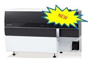
ICP ATOMIC EMISSION SPECTROMETERS

Simultaneous ICP atomic emission spectrometers are next-generation systems that offer the superior accuracy necessary to simultaneously and quickly analyse multiple elements regardless of their concentration levels. They also feature user-friendly software that makes analysis easy. It represent the ultimate in ICP atomic emission spectrometry for environmental, pharmaceutical, food, chemical, metal, and other fields
Specifications
RF Generator
Frequency: 27MHz
RF Power: Max. 1.6kW (0.2 kW step)
RF Device: Transistor
Output Stability: Within ± 0.3%
Efficiency: 75% or better
Spectrometer
Echelle Optics:
Range of wavelength: 167nm to 800 nm
Dispersion elements:
Echelle grating 79 line/mm
Prism
Reciprocal dispersion:
0.21 nm/mm at 200 nm
0.68 nm/mm at 600nm
Resolution:
≤ to 0.005 nm at 200nm
Temperature:
termal controller (38 ℃ )
Atmospheric removal system:
Rotary vacuum pump ≤ 10 Pa
Device
CCD (charge coupled device) detector
Pixel number: 1024 x 1024 pixels (1-inch)
Pixel size: 20μm x 20μm
Cooling control:Peltier device
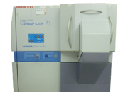
GLOW DISCHARGE PROFILER 
Radio Frequency-Glow Discharge-Optical Emission Spectrometry (RF-GD-OES) from HORIBA can be used on both conductive and non-conductive materials. It can also analyze materials with even surfaces with diameters greater than 4mm. In total, 43 elements, including H, O, N, C and Cl, can be determined by using glow discharge (GD).
Main Application/Advantages
-
The main applications of GD analysis are for surface analysis, bulk analysis and depth profile analysis. For example, GD can be used to profile a Zn-Ni coating.
Specification
Resource
Radio Frequency
Detector
Optical Emission Spectrometer
Sample Shape
Plain, Diameter ≥ 4mm
Detection Limit
ppm (mg/L)
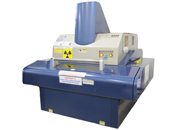
XRF THICKNESS COATING GAUGE 
The XRF Thickness Coating Gauge uses a sensitive, non-contact, and non-destructive method to measure the coating thickness for metallic and non-metallic materials over a range of thicknesses, from as little as 0.05 μm to as much as 70 μm depending on the coating materials.
Main Application/Advantages
The thickness gauge is widely used to determine:
- The thickness of coated materials
-
Elements through spectrum matching
-
Thickness of material in cavities
-
Metallic elements in solutions
Advantages of this gauge include:
-
One-touch focusing operation with laser focus mechanism
-
Automatic measurement functions
-
Thin Film FP software (capable of a wide range of applications including multiple coated layers and Pb free allow coatings)
-
Report creation software (prints out a report of measurement results through macro-enhanced software)
-
Fast, reliable and accurate measurement
Specifications-
Able to determine at least 35 types of electroplated layers; i.e. Au, Ag, Pd, Pd-Ni, Ni-B, Ni-Co, etc.
-
Measures over a wide spectrum of elements from titanium to bismuth
-
Collimator size as small as 0.05mm for smaller measurement areas
-
Please refer to Scanning Electron Microscope