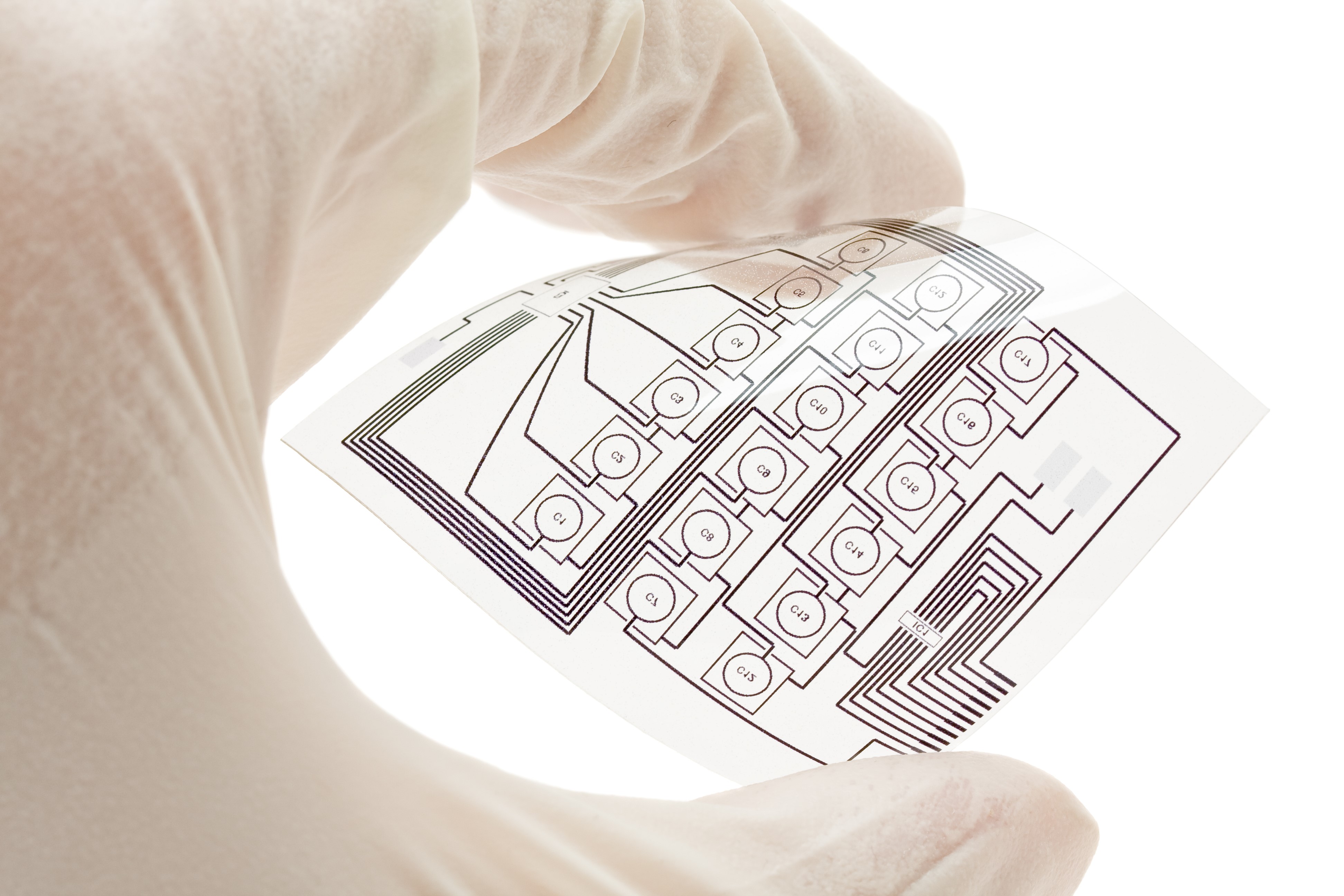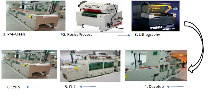
Singapore Epson Plating division specialise in photoetching process with tight tolerances and high repeatability control for substrate that are beyond conventional stamping method's capabilities.The process offer a better cost benefit especially for precision compenents onto various types of material with minimum set up cost.When component integrity is critical, photo etching is often the only suitable metal machining technology as metal temper and magnetic properties are unaffected.
| Photo Etching | ||||||||||||||||||||||||||
 |
We offer wide variety on different substrate material such as Copper Alloys, Beryllium Copper, Stainless Steel, Aluminum, Nickel and Nickel Allous. Silver and Spring steels.Speciality materials suchs as Molydenum, Titanium, Elgiloy, Niobium, Nitino tungsten and SUS can be also etched with intricate details, as well as Polyimide and PET film.
|
|||||||||||||||||||||||||

