
In the semiconductor industry, gold and electroless nickel plating are applied to reflector rings, reflector arrays and top chucks. Gold is used because of its reflectivity, conductivity and heat dissipation qualities. Electroless nickel is valued for its evenness and chemical resistance.
| Under Bump Metalisation (UBM) |
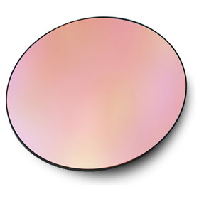 |
For Connecting a Semiconductor Device to the Packaging Substrate.
| Specifications |
| Size: |
4", 6", 8" (Round Wafer) |
| Substrate: |
Ceramic, Al-Si |
| Metallization: |
Ti, Cu, Ni, Au, Ag, Cr |
| Technical Challenges |
| To Provide Excellent Adhesion to Variety of Wafers. |
Metal Diffusion Prevention. |

|
| Plating Technology for Wafers |
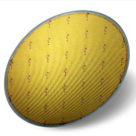 |
Used in LEDs and Semiconductor Wafers in wireless mobile telecommunications technology.
| Specifications |
| Size: |
3", 4", 5", 6", 8" (Round Wafer)
4" (Square Wafer) |
| Substrate: |
Ceramic, Al-Si |
| Metallization: |
Au, Black Ni, Au-Sn, Au-Ni, Si, Cu |
| Thickness: |
0.1 - 100µm |
| Technical Challenges |
Encapsulation Plating on SAW Devices
Copper / Black Nickel Multilayer Plating on (CSSP SAW) Filters Challenges
Encapsulate over the Package, Protecting Against Humidity, Electromagnetic Induction and oxidation.
Intensity of Black is Required as A Detector in Laser Marking. |
Cu Plating on SAW Devices
Copper Plating on SAW Filters
Even Thickness Distribution |
Au-Sn Alloy Plating On Wafer
Limited Chemical Life Span, Color and Composition uniformity |
Wafer Au Plating
Adhesion on Si/Al Alloy Materials, Surface Roughness
Improvement on Roughness and Adhesion using PVD and Electroplating. |
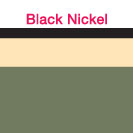
3 Layer Plating on Surface of SAW Device |
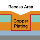
Copper Plating on SAW Filter |
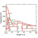
Low Melting Point(280°C – 300°C) |

Good Surface Roughness of Ra = <0.05µm |
Please refer to the relevant pages
Gold Plating,Nickel Plating,Copper Plating,Tin Plating

|
| Plating Technology for RF Packages |
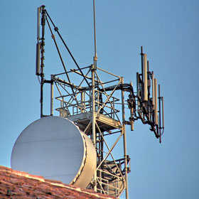 |
RF Packages in Satellites, Base Stations and Other Communication Devices
| Specifications |
| Substrate: |
Ceramic, Cu-Mo, Cu, Cu-W |
| Metallization: |
Ni-Co / Au |
| Thickness: |
1.5 - 3.5µm |
| Technical Challenges |
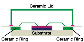
Chip is directly connected to the base |
Plate uniform Au (Ni±0.9μm Au±0.23μm)on 2 different thickness parts which separated by Ceramic.
Selective Lids Plating on New Models of Holy Lids and Ceramics |
Please refer to the relevant pages
Gold Plating,Nickel Plating,Copper Plating

|
![]()
