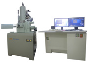
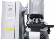
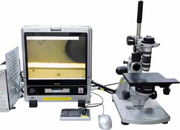
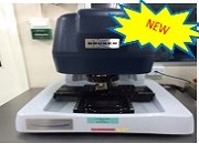
| SCANNING ELECTRON MICROSCOPE | 3D OPTICAL MICROSCOPE | COLOR 3D MICROSCOPE | DIGITAL MICROSCOPES |
SCANNING ELECTRON MICROSCOPE
 Using SEM (scan electron microscope) analysis, the morphology of both conductive and non-conductive materials can be detected when using different detectors SE and BSE, respectively. For EDX analysis, it is possible to check and quantify most elements, except for H, Li and He. There are three types of scanning modes: line analysis, spot analysis and selected area analysis.
Main Application/Advantages
-
With SEM-EDX it is possible to obtain surface morphology, contamination and component, as well as grain size, nodule and cavity, and coating thickness. In particular, a mapping function can be used to identify the distribution of different phases.
Specifications
Cooling System
Liquid Nitrogen
Detector
SE, BSE, ESED
Magnification
30,000x
Resolution
3.0 ~ 4.5nm
The 3D optical microscope combines over three decades of surface metrology innovation and experience from industry partnerships into a single benchtop system to deliver production-ready automation, measurement angle flexibility, outstanding imaging, and proven gage-capable performance. Never before have so many advanced metrology features been available in one benchtop system.
Specifications
Max. Scan Range
> 10 mm
RMS Repeatability (PSI)
<0.03 nm; 0.02 nm typical*
Lateral Resolution
0.38μm min (Sparrow criterion);
0.26μm (with AcuityXR)
Step Height Accuracy
<0.75% **
Step Height Repeatability
<0.1% 1 sigma repeatability
Max. Scan
73μm/sec (with standard camera)
Sample Reflectivity
0.05% - 100%
Max. Sample Slope
Up to 40° (shiny surfaces);
Up to 87° (rough surfaces)
Sample Height
Up to 100mm (4in.) standard;
Up to 150mm (6in.) option
COLOR 3D LASER MICROSCOPE 
The easiest way to perform ultra-precision advanced analysis. It combines the convenience of an optical microscope, SEM and roughness gauge analyses features.
Main Application/Advantages
-
18,000x magnification with Z-axis resolution of 1nm
-
Large depth-of-field comparable to SEMs
-
Several analysis functions, including profile and roughness
-
Nearly 80 degree angle of detection
-
Measures thickness and uniformity of clear layers
-
Non-contact with zero sample preparation
Specifications
Objective lens magnification
10 to 100×
Height measurement
7mm
Display resolution
2048×1536(super fine)1024×768(fine, fast)
Optical zoom
1 to 6×
DIGITAL MICROSCOPES 
Microscopes with the fastest real-time depth composition and 3D functions. Includes integrated 54 Megapixel 3CCD pen-sized camera, 15-inch high-definition LCD monitor and more.
Main Application/Advantages
-
54 Megapixel 3CCD & Actuator
-
Industry's Fastest 3-D Display Function
-
First in Industry, Contrast Optimization
Specifications
Camera Resolution
2 to 54million pixels
LCD monito Size
Color LCD(TFT)15”
LCD Panel size
304.5(H)×228.4(V)mm
LCD Number of pixels
1600(H) ×1200(V)(UXGA)
